JDL – DIODE LAB, BERLIN
PROJECT INFORMATION


| PROJECT | Concept Study New plant for a Diode Production, Berlin |
| OWNER | Jenoptik Diode Lab GmbH |
| CLIENT | Struktur Plan GmbH, Waiblingen |
| ARCHITECT | UNIT4 GmbH & Co. KG, Stuttgart |
| TYPE OF USE | New production facility for semiconductor lasers |
| SERVICE U4 | Conceptual Design |
| DATA BASE | BGF: approx. 7.950 m² Cleanroom Area: ISO 5 + ISO 6 approx. 2.450 m² |
| TIME | 2018 |
| LOCATION | Berlin, Germany |
| PICS | © eikono grafik / UNIT4 GmbH & Co. KG |
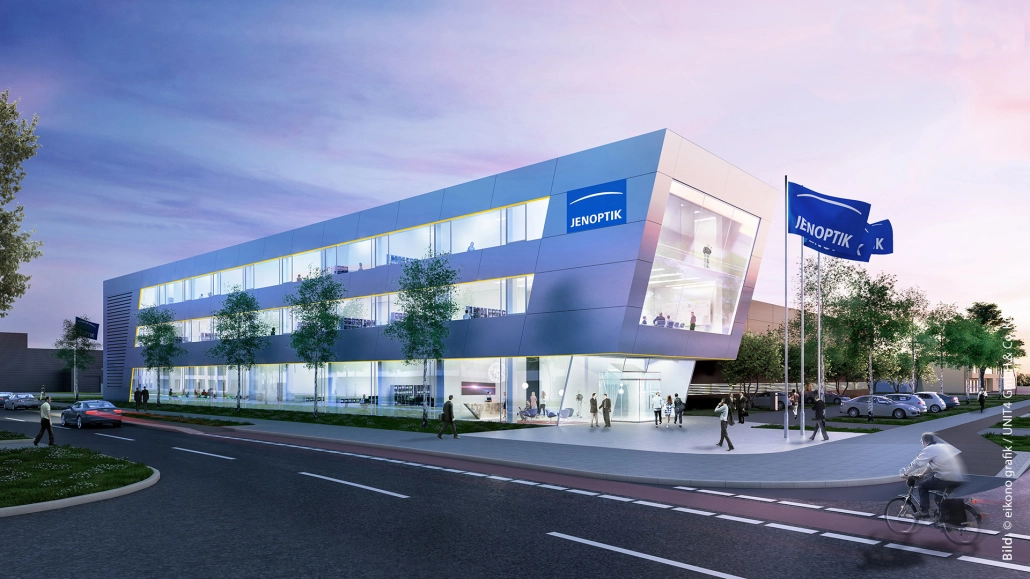
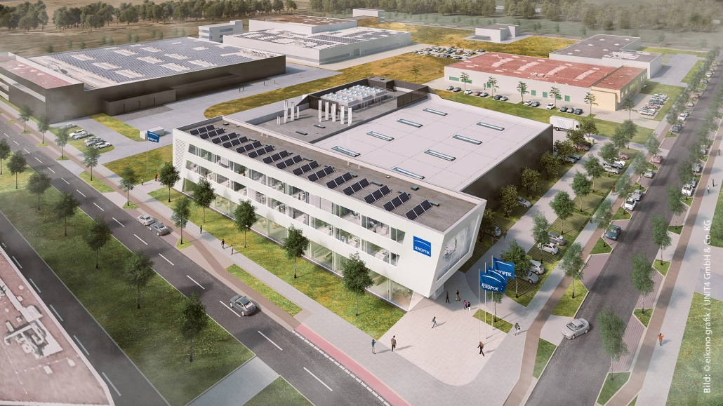
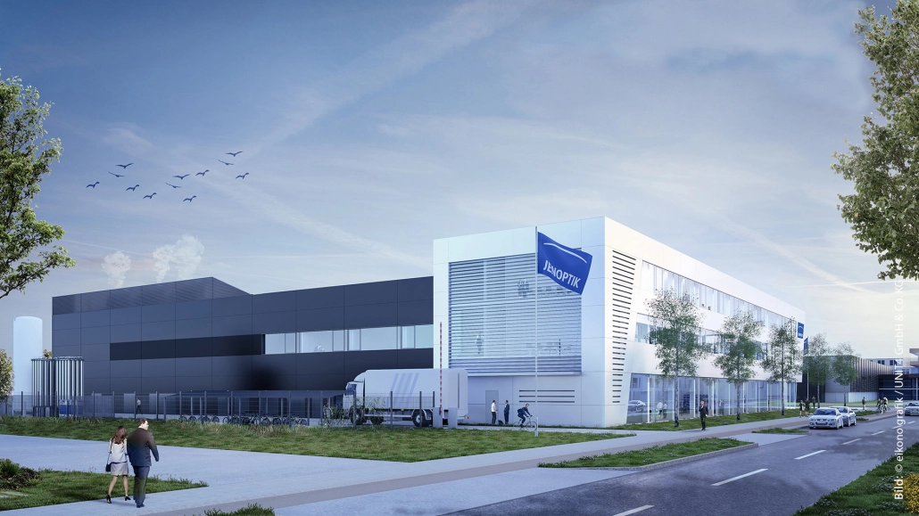
Conceptual Design for a new production facility of semiconductor lasers in Berlin.
In the new manufacturing facility, wafers and semiconductor lasers will be produced in different production steps in class ISO 5 and 6 clean rooms under strict cleanliness requirements. These wafers will be structured and shipped to customers or further processed into high-power diodes for laser devices.